
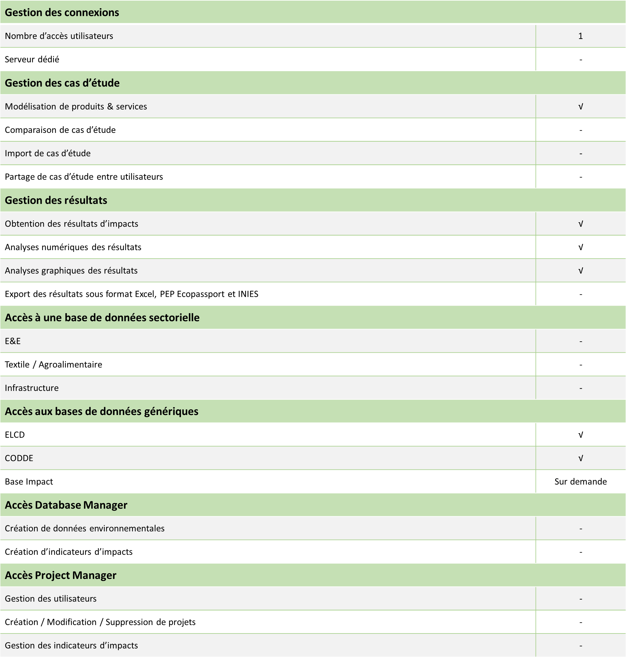
BALANCING PERFORMANCE AND DURABILITY
Microelectronics is a highly dynamic and constantly evolving market. With a constant competition to miniaturize and improve the performance of electronic components, new, ultra-sophisticated production plants are being built.
Many countries are seeking to develop their sovereignty in this key field, with investment programs and R&D support. Among the technological advances, we can cite progress in integrated circuit manufacturing. Lithography, deposition, and etching techniques have been considerably refined to enable the production of ever denser and more efficient circuits. The latest technological advances reach dimensions below 10 nanometers.
However, these advances are generally accompanied by increased environmental impacts: high water consumption, intensive energy use, chemical release, and waste generation.
Faced with these challenges, the microelectronics industry must reconcile technological performance and environmental sustainability.
72% of the world's semiconductor component manufacturing capacity is located in Asia-Pacific (Taiwan, South Korea, China, Japan).

THE INVISIBLE IMPACT OF INTEGRATED CIRCUITS
Like the vital organs of a living being, these essential elements are literally hidden "beneath the surface," hidden from our eyes but essential to the proper functioning of our devices. Their impact, while crucial, thus remains largely invisible to the majority of us.
30%
It is estimated that up to 30% of manufactured wafers may be rejected due to manufacturing defects, quality issues, or insufficient yields. This represents significant quantities of high-purity silicon waste.
80% vs 1%
Take a smartphone, for example. Integrated circuits (microprocessors, memory) account for up to 80% of the carbon footprint, even though they weigh only 1.0% of the smartphone.
x13
Purifying silicon requires up to 13 times more energy than producing aluminum. Silicon is the most widely used element to make wafers.
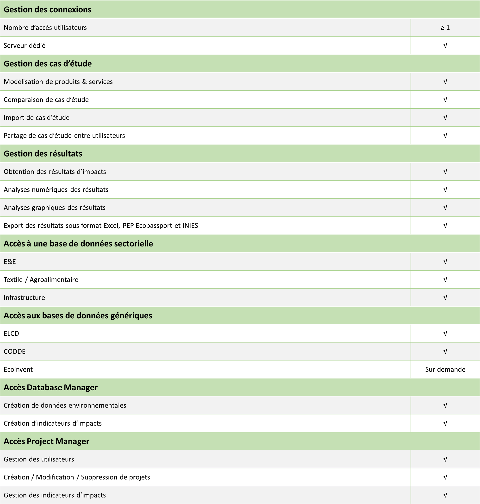
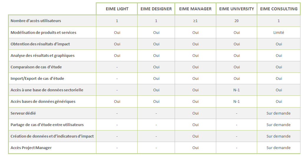
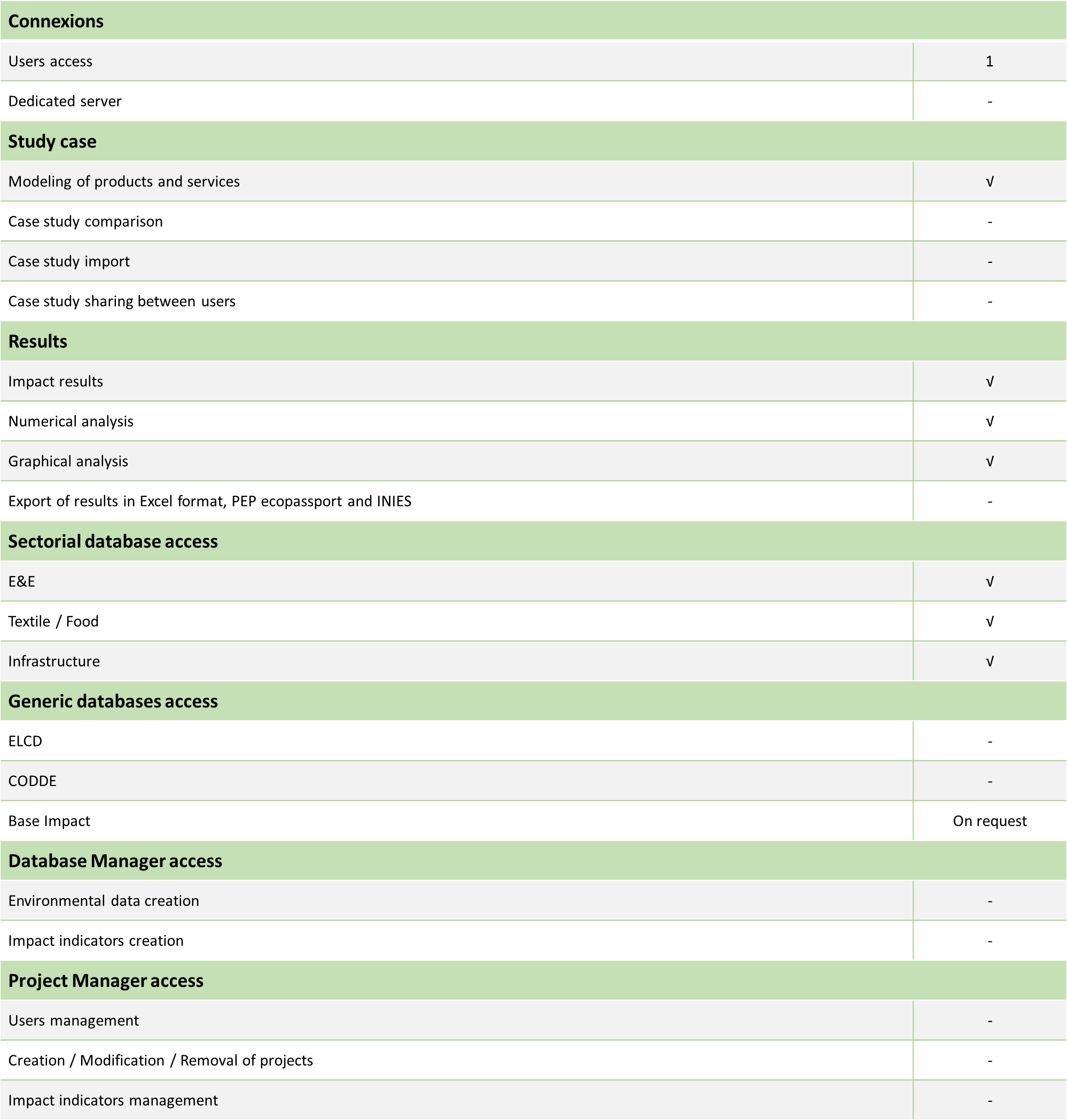
DATASET OVERVIEW

Configurable intetgrated circuits
The MicroElectronics sector database allows you to configure your own integrated circuits:
- Production locations: The user selects from among the 9 countries or 11 available geographical areas.
- Primary quantity: The user enters the total chip area.
- Secondary quantity: The user enters the integrated circuit mass.
- Silicon crystal: The total quantity of silicon crystal (including yields and losses) is automatically calculated by EIME.
- Photolithography: The user enters the number of lithography masks (from 20 to 75) or the etching resolution (from 180 nm to 5 nm).
- Encapsulation: The user selects the package type from among the 13 available (CSP, FW, HI QUAD, LQFP, PDIP, POWSO, SO, SOD, SSOP, TO220, PBGA, TFBGA, VFQFPN).


Production locations
The MicroElectronics sector database covers the 9 countries that design and produce the most integrated circuits. Market data is also available according to 11 geographical areas depending on the technological level of the wafers:
- Countries: China, Taiwan, Korea, Japan, United States, France, Italy, Germany, Netherlands
- Geographic areas:
- Europe, Asia Pacific, Global
- Engraving level: >180 nm, 180-40 nm, 40-20 nm, 20-10 nm, or <10 nm.
By changing the location, the data adapts to the electricity mix of the country concerned (based on IEA data), as well as to the supply and treatment of ultrapure water (based on AquaStat data).

Engraving resolution: from 180 to 5 nanometers
Over the years, etching resolution of silicon wafer has steadily improved, enabling ever-increasing miniaturization of electronic components. Starting with a resolution of 180 nanometers in the 1990s, the integrated circuit industry gradually reduced this scale, reaching 130 nm in the early 2000s, then 90 nm, 65 nm, and 45 nm in the following years. This race for miniaturization has continued, with technology nodes of 32 nm, 22 nm, 14 nm, and even more recently 10 nm and 7 nm. Today, the most advanced technologies are capable of achieving an etching resolution of just 5 nanometers, offering unprecedented integration density and performance for microprocessors, memory devices, and other cutting-edge electronic chips.
The CODDE® database allows you to change the etching level of integrated circuits from 180 to 5 nm.
APPLICATION CASE
Make a difference! Using the CODDE® MicroElectronics database, you can accurately evaluate your products. Here are two application cases developed with EIME:
Production locations
- Package: PBGA
- Component weight: 2,757 mg
- Wafer weight: 40.02 mg
- Etching level: 180 nm (20 masks)
- Production location studied: the 9 countries and 11 geographical areas of the CODDE® database

+55%
Changing the production location can increase the environmental impacts of integrated circuits by +55%.
In this example, the carbon footprint of the component varies from 1.62 kg CO2 eq. (France) to 2.49 kg CO2 eq. (China), a variation of +55%.
- France: 1.62 kg CO2 eq. per component
- Netherlands: 1.98 kg CO2 eq. per component
- ...
- Asia-Pacific: 2.34 kg CO2 eq. per component
- Taiwan: 2.42 kg CO2 eq. per component
- China: 2.49 kg CO2 eq. per component
Engraving resolution
- Package: PBGA
- Component weight: 2,757 mg
- Wafer weight: 40.02 mg
- Engraving levels studied: from 180 nm to 7 nm
- Production location: Worldwide

+267%
Changing the etch level can triple the environmental impacts of integrated circuits.
In this example, the carbon footprint of the component varies from 2.24 kg CO2 eq. (20 masks, >180 nm) to 8.23 kg CO2 eq. (75 masks, 7 nm), a variation of +267%.
- 20 masks, 180 nm: 2.24 kg CO2 eq. per component
- 29 masks, 130 nm: 3.22 kg CO2 eq. per component
- ...
- 54 masks, 22 nm: 5.79 kg CO2 eq. per component
- 58 masks, 14 nm: 6.19 kg CO2 eq. per component
- 75 masks, 7 nm: 8.23 kg CO2 eq. per component


 SFR/Vodafone – Affichage environnemental
 Conforama – Affichage environnemental
 Alstom Transport – Déclarations Environnementales Produit (DEP)
 Schneider Electric – Product Environmental Profile (PEP)
 Atlantic – Product Environmental Profile (PEP)
 Arbor – Fiche Déclarations Environnementale et Sanitaire (FDES)
 Neolife – Fiche Déclarations Environnementale et Sanitaire (FDES)
 Atlantic – Communication Environnementale pour le grand public